FETCH - DECODE - EXECUTE : Revision Notes
The Fetch-Execute Cycle
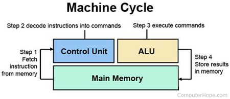
The Fetch-Execute cycle or Fetch-Decode-Execute cycle is also known as the machine cycle (instruction cycle or processor cycle). There are actually four stages to the cycle, the last one being the storing of the result.
- Step 1: An instruction is fetched from the memory address held in the PCR and stored in the CIR. The LMC also fetches the operand (data) at the same time becuase it has a fixed length instruction format.
- Step 2: The current instruction is decoded by the control unit. Remember an instruction is just a (binary) number.
- Step 3: The control unit then sends out signals to the various registers, buses and the ALU required to carry out the instruction, this is the execution.
- Step 4: The final result is stored, either in a register (usually the accumulator) or in RAM.
Main Memory
Main memory is where programs and data are kept when the processor is actively using them. It is connected to the CPU via the front side bus.
Main memory or primary store is usually referred to as RAM or Random Access Memory. "Random" means that the memory cells can be accessed in any order, as opposed the the serial access of magnetic tape. Memory capacity is measured in bytes and computers typically have 4GB (4 billion bytes) or more these days.


A Dual In-line memory Module (DIMM)
Program and Data
The main memory holds the program and data in a single, continuous block (an essential aspect of the Von Neumann architecture. The memory is divided into locations each of which has a unique address which is just a number.
Each address contains an op code or program instruction, such as ADD, and an operand or data. In the case of the LMC the data is always and address of where the value is stored - think of it like a simple variable.
In the Von Neumann architecture op codes and operands are just numbers and there is no way to tell the difference, that is why the program counter is essential.

Assembly language program
Front Side Bus
The front side bus or system bus is the primary connection between the CPU and the rest of the computer (this is where the Von Neumann Bottle-neck would occur if it weren't for the on-board cache memory).
It has three distinct sections: address bus which connects the MAR to the RAM; data bus which connects the MDR to the RAM (and the I/O controllers); control bus which carries control signals from the control unit to the RAM (and the I/O) as well as taking interrupt signals from the hardware back to the control unit.
The address bus is unidirectional while the data bus is bidirectional as data can flow into or out of the MDR. (In the game there is a separate instruction bus connected directly to the CIR which is a feature of a Harvard architecture, although there is only a single memory space shown.
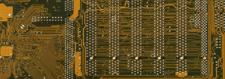
The underside of a motherboard showing PCI bus wiring
Internal Bus
The internal bus connects together all of the registers, the ALU (and Floating Point Unit in modern CPUs). Like the external data bus it is bidirectional allowing data to move between any of the registers (and the ALU). It will operate an order of magnitude faster than the front side bus.
Like the external data bus, the internal bus is a group of wires that run in parallel, a 32-bit CPU will have 32 wires in the bus. You can think of this type of parallel bus like a multi-lane highway which carries large volumes of traffic across many lanes (in this analogy USB is like a high speed rail link - a single but very fast connection carrying data in "single file".
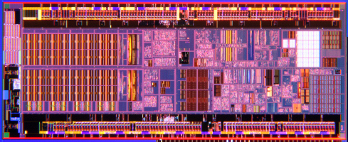
The image to the right shows a close-up of a CPU die, the actual "silicon chip" or integrated circuit of a real CPU. In reality it is less then 1cm wide, so it's impossible to actually see the wiring of the internal bus.
Memory Address Register (MAR)
The MAR is connected to the address bus and always holds the current address that the CPU needs to access, either to read from (e.g. in the LDA instruction) or to write to (e.g. in the STA instruction). During the fetch step of the fetch-execute cycle the MAR will hold a copy of the program counter which is the address of the next instruction to execute.
A good way to picture the MAR is a bit like an address label which tells the Royal Mail delivery person where to deliver an item (equivalent to writing data to an address in memory).
Remember that in the Von Neumann architecture the memory is a continuous block of locations each of which has a unique numeric address (starting at zero). You could picture 4GB of memory like a street with 4 billion houses, each individually numbered, where items can be delivered (or collected).

Think of the MAR like the address label on an envelope
Memory Data Register (MDR)
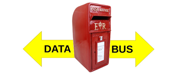
The MDR (sometimes referred to as a memory buffer register) is like a post box that sits between the external data bus and the internal bus through which each instruction and data item must pass.
The MAR (above) tells the memory which address the data item will be read from, or written to.
During the fetch step of the fetch-execute cycle the MDR will get a copy of the next instruction to execute, this will be transferred to the CIR ready to be decoded.
When a value has be fetched from a memory location, as in LDA 007, the address of the value/variable (007 in this case) has to be transferred from the MDR to the MAR and then a second read takes place to load the contents of the memory location into the MDR so the value can be processed - in this case copied to the accumulator.
Program Counter Register (PCR)
The PCR is used to keep track of which instruction (of the program) is currently being processed. This register is vital becuase in the Von Neumann architecture instructions and data are held in the same memory area. Some instructions have no data, most have one item of data and some have more. The PCR is used to keep track of just the instructions as there is no other way to determine whether a number in a memory location is an instruction or not - one of the "disadvantages" of this approach. Remember the Harvard architecture uses separate memory spaces for instructions and data, so this is not an issue.
One way to picture the function of the PCR is to think about how we learn to read, children will tend to use their finger to point to the current sentence they are reading so as not to get lost. The PCR has the same function for the CPU - pointing to the right place in memory.

The PCR allows the control unit to keep track of where it is in the program
Current Instruction Register (CIR)
The CIR will hold a copy of the current instruction or op code that has been fetched from memory (see PCR above). The instruction, which is just a (binary) number will then be decoded by the control unit which will then carry out the steps necessary to execute that instruction - moving data between memory and the MDR, or between the MDR and other registers, or signalling the ALU to carry out a mathematical process such as adding a number (read from memory) to the value in the accumulator.
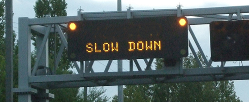
A helpful analogy is an electronic motorway sign (as shown to the right) which can give an instruction to passing motorists, such as slow down (because of bad weather perhaps). The instruction will be loaded onto the sign and the motorists will then control their vehicles appropriately (you hope!) once they have decoded (understood) the instruction.
Status Register
The status register is also known as the condition code register or CCR. This register is updated at the end of each the Von Neumann architecture machine cycle to reflect the outcome of the processing. This information can then be used by a conditional branch instruction such as BRP or BRZ. There are normally four conditions, each represented by an individual bit, often referred to as a flag:
- Z - This indicates that the result of the previous operation was exactly zero.
- N - This indicates that the result of the previous operation was less than zero i.e. negative.
- C - This indicates that the previous operation caused a carry, it generated an extra bit e.g. 10+11=101 in binary, or 01 carry 1, so the carry flag is set to 1.
- V - This indicates that the previous operation caused an overflow - a negative carry (when performing subtraction).

The bits that make up the status register are called flags which can be true or false (1 or 0) to represent the status of the previous calculation e.g. previous result was zero or negative, had a carried bit or cause an over-flow.
Accumulator
The accumulator is the old name for the register that stores the result of calculations carried out by the ALU (see below). Modern CPUs have a number of general purpose registers, any of which can perform the same role as the accumulator.
The definition of the Von Neumann architecture includes the requirement to store the intermediate result of calculations and that is the role of the accumulator. In a simple CPU such as the LMC the accumulator will provide one input to the ALU with the other coming from the MDR. A hidden temporary register will capture the output from the ALU which will then be copied into the accumulator within the same machine cycle.

The accumulator is the CPU's note pad
Arithmetic and Logic Unit (ALU)
The ALU is the part of the CPU that carries out integer calculations, which will include additions, subtractions and logical operations such as AND, OR, NOT and shifting. The CPU in the simple version of this game (and in the LMC) does not provide any logical operations.
Modern CPUs also contain a floating point unit or FPU for short, which can carry out a full range of mathematical operations on real numbers (stored in single or double precision floating point format). A popular metric for CPU performance is FLOPS or floating point operations per second (modern CPUs operate at GFLOPS or Giga-FLOPS while supercomputers are operating at Peta-FLOPS).
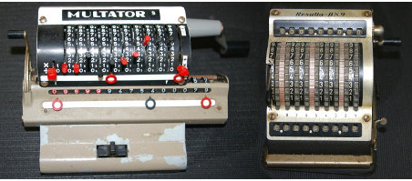
Old mechancial calculators c/o Jim Austin Computer Collection
Control Unit
The control unit coordinates the operation of the CPU. It contains decoding logic and a sequence generator that produces a series of signals (on/off) depending on which instruction is being executed. A sequence generator is based on a simple binary counter circuit (itself built from a collection of flip-flops) combined with additional logic. This is something you'd normally not cover until the first or second year of a computer science degree so don't worry if it sounds terribly complicated.
In this games you get to play the part of the control unit, for each instruction you will have to send signals to the right parts of the CPU in the correct sequence in order to complete execution. But you'll notice that these are simple binary signals, to get something to happen you just click one of the controls. In a CPU that would be a logic signal going from 0 (off) to 1 (on) briefly.

The control unit directs the operation of the CPU
Useful links for further reading:
You can read my e-book about computer architecture on Amazon / Amazon Prime which covers all of this and much more (logic gates, low level programming with the LMC, operating systems, microcontrollers and data types.
The machine cycle explained briefly: https://www.computerhope.com/jargon/m/machcycl.htm [source for image used]
The machine cycle explained very clearly: https://www.futurelearn.com/courses/how-computers-work/0/steps/49284
The different categories of memory: https://www.computerhope.com/jargon/m/memory.htm
The different types of RAM: https://uk.crucial.com/articles/about-memory/different-types-of-memory-explained
The LMC: https://en.wikipedia.org/wiki/Little_man_computer
Low level programming / machine code: https://medium.com/coderscorner/machine-code-dd8fcbe3153
Computer buses explained: https://www.computerhope.com/jargon/b/bus.htm
Why do we call it a bus? https://en.wikipedia.org/wiki/Busbar
Computer bus in detail, with some history: https://zappedia.com/external-data-bus/
Video about computer bus: https://www.youtube.com/watch?v=7QffiMyMpnM
Special registers: https://www.geeksforgeeks.org/different-classes-of-cpu-registers/
CPU registers: http://digitalthinkerhelp.com/what-is-cpu-processor-register-in-computer-its-types-with-functions/ (Note: this page defines MBR and MDR, but they're just different names for the same thing!)
Arithmetic and Logic Unit: https://arith-matic.com/notebook/arithmetic-logic-unit-introduction
Arithmetic and Logic Unit definition: https://www.britannica.com/technology/arithmetic-logic-unit
Control Unit, a technical description: https://www.geeksforgeeks.org/introduction-of-control-unit-and-its-design/
Control Unit - hardwired vs microcoded: https://www.elprocus.com/what-is-control-unit-components-its-design/
If you have any suggestions for useful links or any feedback on the game please email me: Richard at With Hindsight (UK)
Copyright © 2021 R.J.Hind / With Hindsight
